Difference Between SMD Soldering and DIP Soldering
Modern electronics manufacturing relies on two main soldering techniques: SMD (Surface Mount Device) soldering and DIP (Dual In-line Package) soldering. These methods not only differ in their technical approach but also in the components they use, their applications, and the advantages they offer.
Understanding the distinctions between SMD and DIP soldering is essential for engineers, manufacturers, and electronics enthusiasts. This article explores the core differences, methods, and use cases of both techniques in detail.

SMD Components and Soldering Overview
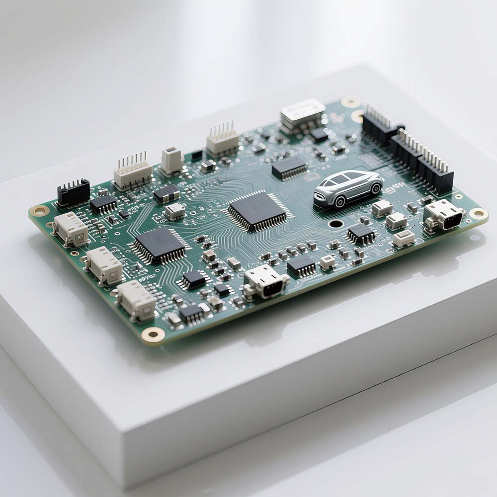
SMD components are designed to be mounted directly onto the surface of printed circuit boards (PCBs). They have no leads or very short leads, which reduces parasitic inductance and capacitance, making them ideal for high-speed and high-frequency circuits. Common types of SMD components include resistors, capacitors, diodes, LEDs, transistors, and integrated circuits.
Due to their small size and absence of leads that pass through the PCB, SMD components allow designers to place components on both sides of a PCB, increasing functional density and minimizing circuit footprint. This is crucial in modern electronics where space-saving is a priority.
SMD Soldering Methods and Process
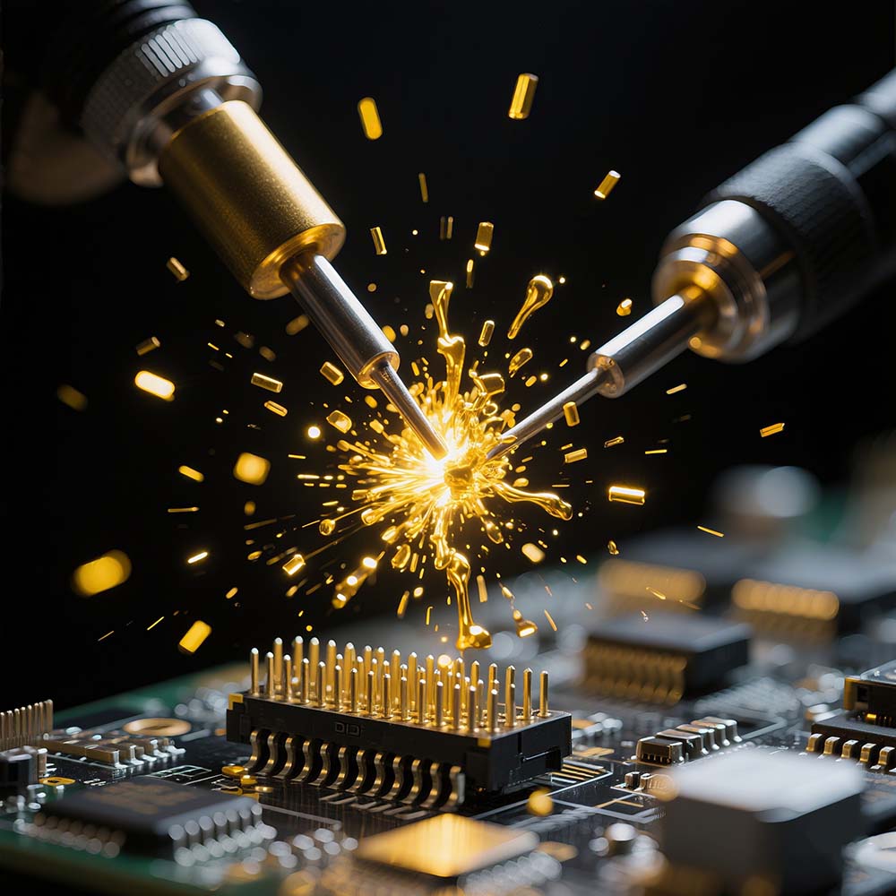
The primary method for soldering SMD components is reflow soldering. In this process, solder paste is applied to the PCB pads using a stencil, components are placed with automated pick-and-place machines, and then the board is passed through a reflow oven where the solder melts to form permanent joints.
For rework or small production runs, hot air soldering and hand soldering using fine-tipped irons and tweezers may be used. After soldering, inspection using automated optical or X-ray systems ensures the quality of the connections.
Advantages and Disadvantages of SMD Soldering
The major advantages of SMD soldering are its compact design capabilities, high component density, and suitability for automated, high-volume production. SMD components offer better performance in high-frequency applications and enable lightweight and portable device designs.
However, the small size of SMDs makes manual handling challenging, and they are not ideal for high-power applications or environments with mechanical stress. The equipment needed for accurate placement and soldering can also be costly.
Applications of SMD Technology
SMD components are ubiquitous in modern electronics. They are widely used in smartphones, tablets, laptops, networking equipment, automotive electronics like engine control units (ECUs), wearable devices, and embedded systems. Their space-saving and performance characteristics make them indispensable in any field that demands miniaturization and efficiency.
DIP Components and Soldering Overview
DIP components feature two parallel rows of metal pins, designed to be inserted into holes drilled into the PCB. Once in place, these pins are soldered to pads on the underside of the board. This through-hole mounting provides a strong mechanical and electrical connection.
Common DIP components include microcontrollers, logic ICs, voltage regulators, operational amplifiers, and power transistors. Due to their larger size, these components are easy to insert, align, and solder manually, making them ideal for prototyping and educational purposes.
DIP Soldering Methods and Process
Wave soldering is the primary method for soldering DIP components in medium to high-volume production. In this process, a PCB populated with through-hole components passes over a wave of molten solder, which adheres to the exposed metal leads and pads to form connections.
Manual soldering, using a soldering iron, is also widely used for low-volume assemblies, repairs, or projects requiring customization. After soldering, excess leads are trimmed and joints are visually inspected.
Advantages and Disadvantages of DIP Soldering
DIP soldering offers simplicity and mechanical strength. It’s easier to inspect, repair, and prototype using DIP components due to their size and through-hole structure. They provide strong joints that can handle mechanical stress better than SMD components.
However, DIP components take up more board space, making them unsuitable for compact designs. They are also less compatible with automation and tend to increase production costs and time in mass manufacturing settings.
Applications of DIP Technology
Despite the rise of SMDs, DIP components remain prevalent in specific applications. They are found in power supplies, industrial automation controllers, test equipment, vintage or legacy hardware, and educational kits. Many hobbyist and DIY electronics projects also prefer DIP components for their ease of use.
Comparing Reflow vs. Wave Soldering
Reflow soldering and wave soldering serve distinct purposes based on the components used.
Reflow soldering is optimized for SMDs, providing precise temperature control and compatibility with high-density designs. It allows for both sides of a PCB to be populated and soldered, which is crucial for modern consumer and industrial electronics. The process is clean, efficient, and ideal for miniaturized devices.
Wave soldering, by contrast, is best suited for through-hole components. It is faster than manually soldering each pin and provides consistent results. However, it’s less suitable for compact electronics or SMDs unless special techniques are used to combine both component types on the same board.
While reflow soldering requires a reflow oven, solder paste, and stencil application, wave soldering demands flux application, preheating, and controlled immersion in molten solder.
The Difference Between SMD and DIP Components
The primary difference between SMD and DIP components lies in their mounting style. SMD components are mounted directly onto the PCB surface, allowing for smaller and more complex designs. DIP components are inserted through holes in the PCB and soldered on the opposite side, providing a mechanically robust connection that is easier to handle manually.
SMD components are designed for automated production and high-performance circuits. DIP components, while bulkier, are easier to work with for prototyping, educational use, and rugged applications that demand mechanical strength.
Selecting between SMD and DIP components depends on the application’s requirements: size constraints, production volume, performance needs, and available equipment all play a role.
Conclusion
Both SMD and DIP soldering play a vital role in electronics manufacturing. SMD soldering dominates modern high-speed, compact, and mass-produced electronics due to its efficiency and miniaturization capabilities. It is favored in commercial consumer electronics, telecommunications, and embedded systems where space, performance, and automation are important.
On the other hand, DIP soldering remains highly valued in prototyping, educational environments, and high-durability applications. Its ease of use and strong mechanical connection make it ideal for testing circuits, DIY electronics, and repairs.
Understanding the difference between SMD and DIP soldering can help engineers and designers make informed decisions. Whether you are assembling a high-frequency, compact IoT device or prototyping a durable industrial control circuit, choosing the right component type and soldering method is critical to achieving reliable, efficient, and cost-effective results.